From breadboard to my first PCB
Last time I had the four-transistor valve circuit working on a breadboard. It flips the CWX-15Q open and closed from one switch and cuts the motor at the limit switches, which is the whole trick.
A breadboard is not a thing I want to mount near plumbing at a summer house, though. So this seemed like as good a time as any to do something I'd never actually done before: make my own PCB.
Off the breadboard
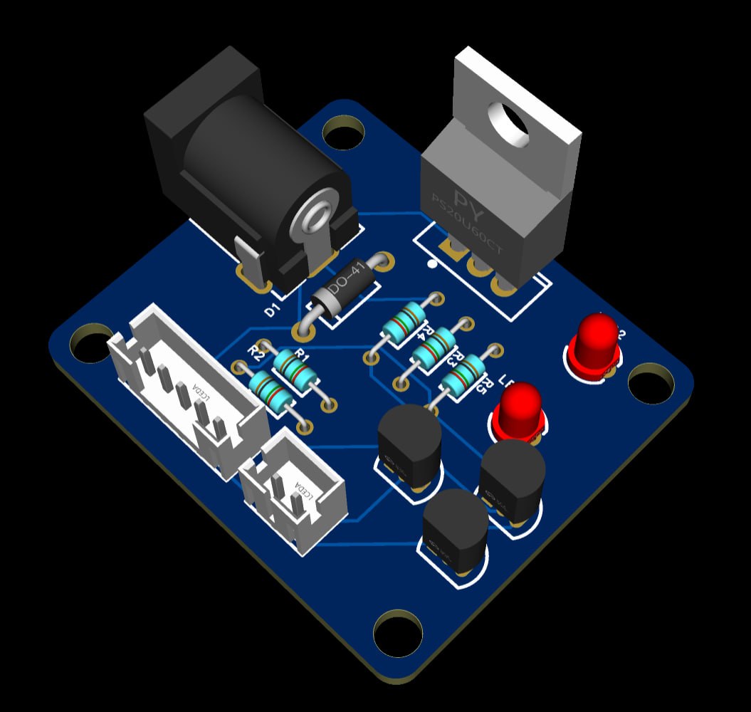
I sketched the schematic in EasyEDA. Nothing exotic — it's the same circuit from the breadboard, just drawn properly: Q1, an IRF610, is the power MOSFET that switches the motor; Q2–Q4 are little 2N7000s doing the run-and-stop logic; R3–R5 are the 10K gate resistors; and a pair of 470 Ω LEDs show which way the valve was last sent. Power comes in on a 12 V barrel jack, the switch lands on a 2-pin JST, and the valve's five CR05 wires land on a 5-pin JST.
I deliberately kept everything through-hole. I wanted to hand solder this one — partly because it's my first board and I'd rather not fight a hot-air station and a reel of 0402s on day one, and partly because through-hole parts are easy to probe, desolder, and swap when (not if) I got something wrong.
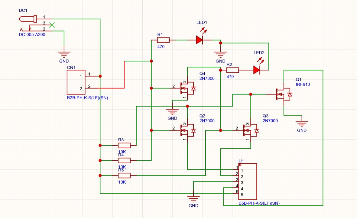
Two things Claude caught
I did a fair amount of back-and-forth with Claude on the design before ordering, and it caught two mistakes that would each have cost me a board.
The first was a dumb wiring error. While I was tidying and simplifying the schematic, I'd connected the trace from the switch to the supply rail instead of to ground. Easy to do, hard to spot once the schematic gets busy, and exactly the kind of thing you don't notice until the board is in your hand and nothing works. Claude flagged it on a read-through and I moved it back to GND.
The second was more educational. My first cut had no protection across the motor at all. The motor is an inductive load, and when the MOSFET switches it off the collapsing field dumps its energy as a back-EMF spike — a voltage kick that can punch straight through the FET. The fix is a flyback diode (D1) across the motor: in normal running it does nothing, but the instant the current is cut it gives that inductive kick a harmless loop to circulate in instead of frying Q1.
Full disclosure: that explanation is Claude's, not mine. I added the diode because it told me to, and I've reproduced its reasoning here — but I still don't really understand it well enough to have arrived at it on my own.
Parts on the board
| Ref | Part | Role |
|---|---|---|
| Q1 | IRF610 | Power MOSFET — switches the 12 V motor |
| Q2–Q4 | 2N7000 ×3 | Small-signal MOSFETs — the run/stop logic |
| D1 | Diode (DO-41) | Flyback clamp across the motor |
| R1, R2 | 470 Ω ×2 | LED current limiting |
| R3–R5 | 10K ×3 | Gate resistors |
| LED1, LED2 | 3 mm LED ×2 | Last-commanded-direction indicators |
| DC1 | DC-005 barrel jack | 12 V power in |
| CN1 | 2-pin JST PH | Switch |
| U1 | 5-pin JST PH | Valve (CR05: 2 motor + 3 limit-switch wires) |
Laying it out and sending it off
With the schematic fixed I did the layout. It's a single-sided sort of board in spirit — a handful of parts, generously spaced, no attempt to be clever about size. First boards are for learning the toolchain, not for setting density records.
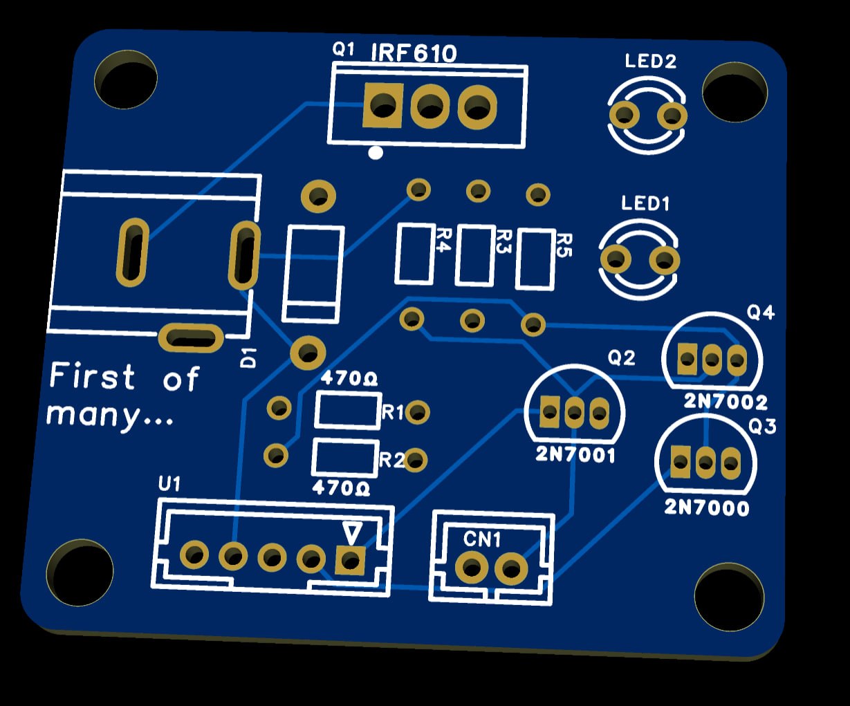
I sent it to PCBWay — five boards, about $10 with shipping, minus a $5 coupon, so call it five dollars to hold my first real PCB. The soldermask is the default blue. And yes, I put "First of many…" on the silkscreen, because if it isn't, I've wasted a perfectly good corner.
What's next
The boards aren't here yet. When they arrive I'll stuff and solder one, then put it on the bench with the valve and confirm it behaves the same as the breadboard did — open, stop, closed, stop.
After that it's an enclosure and the actual install at the summer house, with the switch somewhere I can reach standing up.
Same caveat as last time, plus a new one: this still hasn't met a Swedish January or any actual water — and now it hasn't even met a soldering iron. Everything above is renders. Wi-Fi is still firmly behind the rule that the dumb version has to survive a winter first.